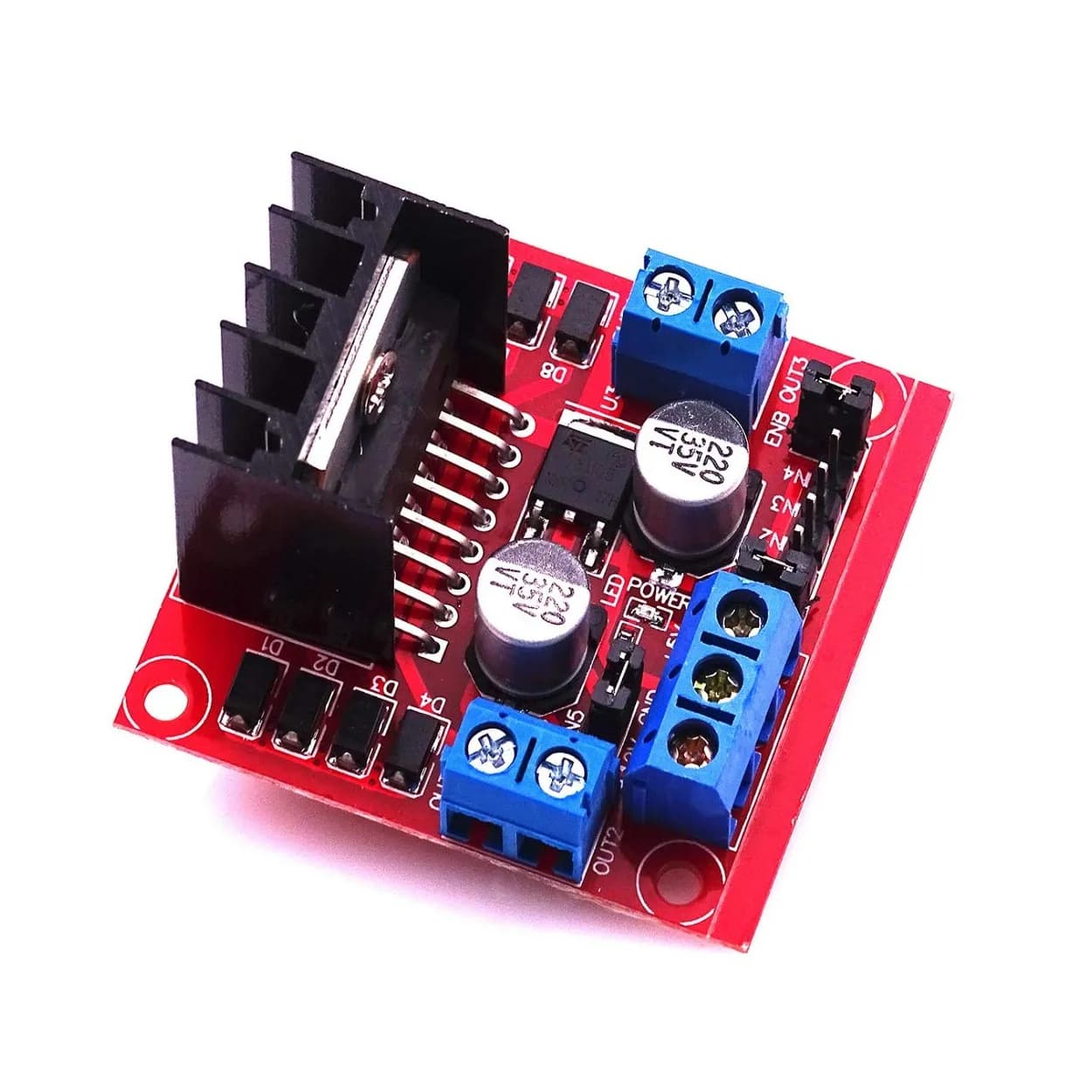
Advanced PCB Design Architecture: High-Speed Routing, Signal Integrity, and DFM
Master advanced custom PCB design techniques covering layer stackup engineering, high-speed signal integrity, power distribution network optimization, and manufacturing rules.

Designing custom Printed Circuit Boards (PCBs) for modern electronics requires moving far beyond basic schematic capture and simple trace autorouting. As system clock frequencies increase, rise times shrink into the sub-nanosecond domain, and component densities rise, physical PCB traces cease to act as simple electrical connections. Instead, they behave as distributed transmission lines susceptible to noise, crosstalk, ground bounce, and parasitic inductance.
This guide explores the advanced engineering principles required to design high-performance, custom PCBs. It covers layer stackup planning, impedance matching, power distribution network (PDN) design, signal integrity (SI), and Design for Manufacturability (DFM) guidelines essential for taking a concept to production-ready hardware.
Layer Stackup Architecture and Controlled Impedance
The board stackup is the foundation of any multi-layer PCB design. A poorly planned stackup leads to unmanageable Electromagnetic Interference (EMI), signal distortion, and physical board warping during reflow soldering.
Stackup Symmetry and Layer Selection
When moving from 2-layer designs to 4, 6, or 8+ layer stackups, maintaining structural symmetry around the center dielectric core is critical to prevent mechanical bowing and twisting (per IPC-6012 standards).
For a typical 4-layer high-speed board, the preferred stackup places inner reference planes between outer signal layers:
- Top Layer: High-speed signals / Component placement
- Inner Layer 1: Solid Ground Plane (GND)
- Inner Layer 2: Power Plane (PWR) or split power rails
- Bottom Layer: Low-speed signals / Auxiliary routes
For complex high-density interconnect (HDI) boards, a 6-layer stackup provides significantly better signal integrity by offering adjacent reference planes for all signal layers:
| Layer | Type | Dedicated Function |
|---|---|---|
| L1 | Signal | High-speed critical signals (Microstrip) |
| L2 | Ground | Continuous return path reference plane |
| L3 | Signal | Inner strip-line routing layer |
| L4 | Power / Ground | Power plane or secondary reference plane |
| L5 | Ground | Secondary return path reference plane |
| L6 | Signal | General routing and power distribution |
Controlled Impedance Modeling
High-speed traces must be modeled as transmission lines when the trace length exceeds one-sixteenth of the signal's fast rise-time wavelength ($\lambda / 16$). Standard target single-ended characteristic impedance ($Z_0$) is usually $50,\Omega$, while differential impedance ($Z_{diff}$) is typically $90,\Omega$ (USB), $100,\Omega$ (Ethernet, PCIe), or $85,\Omega$ (DDR memory).
Characteristic impedance for a surface microstrip is calculated using the modified IPC-2141 formula:
$$Z_0 = \frac{87}{\sqrt{\epsilon_r + 1.41}} \ln\left( \frac{5.98h}{0.8w + t} \right)$$
Where:
- $\epsilon_r$ is the relative dielectric permittivity of the substrate material (e.g., $4.2$ to $4.5$ for standard FR-4).
- $h$ is the dielectric height above the reference plane.
- $w$ is the trace width.
- $t$ is the trace copper thickness.
Engineers must specify exact trace geometries in their EDA software (such as KiCad, Altium Designer, or Cadence Allegro) based on the specific dielectric thickness provided by the chosen PCB fabricator.
Signal Integrity and High-Speed Routing Strategies
Ensuring signal integrity involves controlling reflections, minimizing capacitive and inductive crosstalk, and maintaining clear signal return paths across the layout.
Microstrip Geometry (Top Layer Signal over GND):

     +-----------------------+  <-- Trace (Width: w, Thickness: t)
=====|                       |============================= Top Copper
     +-----------------------+
-----------------------------------------------------------
     Dielectric Substrate (Permittivity: Er, Height: h)
-----------------------------------------------------------
=========================================================== Solid Ground Plane
Uninterrupted Ground Return Paths
Every signal current flowing through a trace returns to its source through the path of least impedance. At frequencies above a few hundred kilohertz, the path of least impedance lies directly beneath the signal trace on the adjacent reference plane.
- Avoid Plane Splits: Never route high-speed traces across gaps or splits in reference ground planes. Crossing a plane split forces the return current to take a large loop around the obstacle, generating severe radiative EMI and high inductive ringings.
- Stitching Vias: When a signal changes layers, its return current must change reference planes. Place stitching vias directly adjacent to signal transition vias when switching between ground planes.
Differential Pair Routing
Differential signaling (e.g., LVDS, USB, HDMI) relies on equal and opposite signals running along closely coupled traces.
- Intra-Pair Length Matching: Keep length mismatch within strictly tight tolerances (e.g., $< 0.15\text{ mm}$ for USB 2.0; $< 0.05\text{ mm}$ for PCIe Gen 3) using serpentine tuning runs near the point of divergence.
- Symmetrical Phase Matching: Place length-compensating bends as close to the source of asymmetry as possible.
- Constant Coupling: Maintain uniform edge-to-edge spacing ($s$) along the entire differential route. Avoid separating traces around pads or mechanical obstructions.
Crosstalk Mitigation Rules
Crosstalk occurs via capacitive and inductive coupling between parallel traces.
- The 3W Rule: Spacing between trace centers should be at least three times the trace width ($3W$) to reduce crosstalk field coupling by roughly 70%. For aggressive high-speed buses, extend spacing to $5W$.
- Orthogonal Layer Routing: Route adjacent signal layers perpendicular to one another (e.g., Layer 1 horizontal, Layer 3 vertical) to prevent broadside coupling.
Power Integrity (PI) and Decoupling Architectures
Power Integrity focuses on delivering clean, stable direct-current (DC) voltage to active ICs while suppressing dynamic switching noise across the Power Distribution Network (PDN).
Target Impedance and Decoupling Capacitor Arrays
An ideal PDN presents an impedance lower than a maximum target impedance ($Z_{target}$) across a wide frequency range:
$$Z_{target} = \frac{\Delta V_{ripple}}{I_{step}}$$
Where $\Delta V_{ripple}$ is the maximum allowable voltage ripple (e.g., $3%$ of $1.8\text{V} = 54\text{ mV}$) and $I_{step}$ is the peak dynamic switching current of the load.
To maintain low target impedance from low frequencies up to several hundred megahertz, use a multi-tiered array of surface-mount Ceramic Capacitors (MLCCs):
       Broadband PDN Decoupling Strategy

Impedance
   ^
   |      Bulk Cap           Mid-Range MLCC          Ultra-Low ESL MLCC
   |     (10uF - 100uF)       (100nF - 1uF)           (10nF - 100nF)
   |        \                      |                     /
   |         \                     |                    /
   +----------\--------------------|-------------------/-------- Z_target Line
   |           \                   |                  /
   +-------------------------------------------------------------> Frequency
- Bulk Decoupling ($10,\mu\text{F} - 100,\mu\text{F}$): Handles low-frequency load transients (100 kHz – several MHz).
- Local High-Frequency Decoupling ($100\text{ nF}$ and $10\text{ nF}$): Placed directly adjacent to power pins of ICs to supply ultra-fast current spikes. Choose low Equivalent Series Inductance (ESL) packages (e.g., 0402 or 0201).
Mounting Inductance Minimization
The effectiveness of a decoupling capacitor is limited by its mounting loop inductance—the inductance formed by the tracks, vias, and internal plane spacing connecting the capacitor to the IC.
- Place vias as close to the capacitor solder pads as fabrication tolerances permit.
- Prefer wide, short trace segments over long narrow traces for capacitor ground/power taps.
- Use side-by-side via placement or "via-in-pad" technology (plated flat) to minimize loop area.
Thermal Management & Mechanical Layout Considerations
High-power components like microprocessors, switching regulators (SMPS), and motor drivers require active thermal design strategies to keep junction temperatures ($T_J$) below critical limits.
Thermal Via Arrays under Exposed Thermal Pads
For components utilizing exposed bottom ground pads (QFN, HTSSOP, BGA packages), heat must be conducted down through the PCB layers to copper planes:
- Grid Spacing: Implement a thermal via matrix directly within the component ground pad using a grid pitch of $1.0\text{ mm} - 1.2\text{ mm}$.
- Via Sizing: Use small drill diameters ($0.3\text{ mm}$) to prevent excessive solder wicking during reflow assembly if vias are not plugged/capped.
- Copper Thickeners: Utilize outer copper weights of 2 oz/ft² ($70,\mu\text{m}$) on layers carrying sustained current over $3\text{ A}$.
$$R_{\theta,via} \approx \frac{h}{k_{Cu} \cdot \pi (r_{outer}^2 - r_{inner}^2)}$$
Where $k_{Cu}$ is thermal conductivity of copper ($\approx 385\text{ W/m}\cdot\text{K}$), $h$ is PCB thickness, and $r$ represents via wall boundaries.
Design for Manufacturability (DFM) and Fabrication Prep
Creating a functional layout is only half the battle; the design must be manufacturable at scale with acceptable yields. Adhering to DFM rules avoids costly re-spins and manufacturing delays.
IPC Standards Baseline
Always align layout tolerances with industry standard IPC specifications:
- IPC-2221: Generic Standard on Printed Board Design.
- IPC-7351: Generic Requirements for Surface Mount Design and Land Pattern Standard.
- IPC-A-600 / IPC-A-610: Acceptability of Printed Boards and Electronic Assemblies.
Essential Fabrication Clearances
Verify that layout design rules (DRC) enforce realistic limits relative to the capability matrix of your PCB fabricator:
| Parameter | Standard Class 2 (Low Cost) | Advanced HDI / Class 3 |
|---|---|---|
| Min Trace / Space | 6 mil / 6 mil ($0.15\text{ mm}$) | 3 mil / 3 mil ($0.075\text{ mm}$) |
| Min Via Drill Size | 12 mil ($0.3\text{ mm}$) | 4 mil ($0.1\text{ mm}$ Microvia) |
| Minimum Annular Ring | 5 mil ($0.125\text{ mm}$) | 3 mil ($0.075\text{ mm}$) |
| Solder Mask Clearance | 2 mil ($0.05\text{ mm}$) | Direct On-Pad (0 clearance) |
| Board Edge Clearance | 10 mil ($0.25\text{ mm}$) | 15 mil ($0.38\text{ mm}$) |
Thermal Relief vs. Direct Connections
- Hand Soldering / Repairability: Connect component pins to copper pours using thermal relief spokes (cross-hatched connections) to limit heat dissipation into the copper plane during assembly.
- High-Current Connections: Use direct solid fills on power components where maximum thermal and electrical conductivity is required, keeping in mind that automated reflow ovens will be necessary.
Gerber Generation, Verification, and Fabrication Handoff
Before releasing a design to production, complete a final design verification process:
1. Execute Complete DRC Check
Run automated Design Rule Checks in your EDA tool with zero permitted errors or unacknowledged warnings. Verify clear net connections, minimum annular ring compliance, trace-to-trace spacing, and unrouted net checks.
2. File Format Output Selection
Generate production output files in modern, robust formats:
- ODB++ or Gerber X2: Strongly preferred over legacy Gerber RS-274X. Gerber X2 and ODB++ natively embed layer stackup information, drill attributes, netlists, and component placement data, dramatically reducing fabrication errors caused by manual interpretation.
- NC Drill Files: Ensure drill origin matches the Gerber coordinate origin. Use standard absolute coordinate mapping.
3. Fabrication & Assembly Drawings
Provide comprehensive documentation packages including:
- Detailed layer stackup diagram showing dielectric materials, target layer thicknesses, and copper weights.
- Drill map chart detailing hole counts, finished hole sizes, and tolerances (+/- 2-3 mil).
- Bill of Materials (BOM) linked to manufacturer part numbers (MPN), land patterns, and designators.
- Pick-and-Place centroid files (
.csvor.txt) with accurate X-Y coordinates, layer assignments, and rotational orientation according to IPC-7351 rules.
Summary Checklist for Advanced PCB Design
- Stackup First: Define layer order, ground reference planes, and trace widths for target differential/single-ended impedance prior to routing.
- Ground Continuity: Keep reference ground planes intact; never cross splits with high-speed signals.
- Decouple Closely: Minimize trace/via loop inductance between decoupling MLCC pads and component power pins.
- Thermal Dissipation: Include via arrays beneath high-power components and specify sufficient copper weights.
- DFM Verification: Validate design rules against real-world fab shop limitations and export rich manufacturing data (ODB++ or Gerber X2).
By applying these disciplined PCB engineering methodologies, hardware designers can build robust, highly reliable circuit boards that function correctly on the first revision—preventing costly re-spins and long troubleshooting delays.